Giornate Sulla Termoelettricità 2022 - Book Of Abstracts 16 - 17 FEBBRAIO
←
→
Trascrizione del contenuto della pagina
Se il tuo browser non visualizza correttamente la pagina, ti preghiamo di leggere il contenuto della pagina quaggiù

Giornate
 Sulla
 Termoelettricità
 2022

Book Of Abstracts

16 – 17 FEBBRAIO

PISA
Scuola Normale Superiore

 1
2

Indice
Organizzazione 4
 Comitato Scientifico 4
 Comitato Organizzatore 4
Informazioni e collegamenti 5
Programma 6
 Mercoledì 16 febbraio 2022 6
 Giovedì 17 febbraio 2022 8
Contributi 10
 INVITED LECTURE 11
 SESSIONE 1: Thermoelectric generators and devices (I) 13
 SESSIONE 2: Thermoelectric materials: design and characterization 19
 SESSIONE 3: Thermoelectrics in enterprise applications 25
 SESSIONE 4: Computational approaches to materials design and investigation 28
 SESSIONE 5: Thermoelectric generators and devices (II) 39
Indice degli autori 42

 3
Organizzazione
Associazione Italiana di Termoelettricità
Scuola Normale Superiore
CNR-ICMATE
Università di Modena e Reggio Emilia

Comitato Scientifico

C. Artini - Università di Genova
S. Boldrini - CNR-ICMATE, Padova
A. Castellero - Università di Torino
R. Carlini - LA Klee-Barabino, Genova
V. Demontis - Scuola Normale Superiore
M. Fabrizio - CNR-ICMATE, Padova
A. Famengo - CNR-ICMATE, Padova
C. Fanciulli - CNR-ICMATE, Lecco
A. Ferrario - CNR-ICMATE, Padova
E. Guidi - Scuola Normale Superiore
D. Narducci - Università di Milano Bicocca
G. Pennelli - Università di Pisa
D. Prete - Scuola Normale Superiore
F. Puglia - ISC srl
A. Rizzo - Enea, Brindisi
F. Rossella - Università di Modena e Reggio Emilia

Comitato Organizzatore

V. Demontis - Scuola Normale Superiore
E. Guidi - Scuola Normale Superiore
D. Prete - Scuola Normale Superiore
F. Rossella - Università di Modena e Reggio Emilia
A. Ferrario - CNR-ICMATE, Padova

 4

Informazioni e collegamenti
Portale dell'Associazione Italiana di Termoelettricità
http://ait.icmate.cnr.it
Scuola Normale Superiore
http://www.sns.it/
Scuola Normale Superiore - NEST
http://www.laboratorionest.it/
CNR-ICMATE - Istituto di Chimica della Materia Condensata e di Tecnologie per l'Energia
http://www.icmate.cnr.it
CNR-NANO – Istituto Nanoscienze
http://www.nano.cnr.it
Università di Modena e Reggio Emilia
http://www.unimore.it

 5
Programma

Mercoledì 16 febbraio 2022

10:00 Registrazione dei partecipanti

10:30 Benvenuto istituzionale e introduzione del presidente dell’AIT

Invited lecture

10:50 Simone Fabiano - Linköping University, Sweden
 Unconventional thermoelectric materials for energy harvesting and
 sensing application

Sessione 1: Thermoelectric generators and devices (I)
Chair: Francesco Rossella

11:50 Elisabetta Di Maggio - Università di Pisa
 Thermoelectric devices based on nanostructured silicon, the ideal
 material for thermoelectric applications

12:10 Federico Giulio - Università degli Studi di Milano-Bicocca
 Exceptional thermoelectric power factor in hyperdoped, fully
 dehydrogenated nanocrystalline silicon thin film

12:30 Valeria Demontis - Scuola Normale Superiore di Pisa
 Drastic reduction of thermal conductivity in InAsSb periodic twinning
 nanowires

12:50 Giovanni Pennelli - Università di Pisa
 Electrical and thermal optimization of energy-conversion systems based
 on thermoelectric generators

13:10 - 14:30 Pranzo

 6
Sessione 2: Thermoelectric materials: design and characterization
Chair: Valeria Demontis

14:30 Cristina Artini - Università di Genova/CNR ICMATE
 Effects of deposition and annealing temperature on the electrical
 properties of skutterudite Smy(FexNi1-x)4Sb12 thin films

14:50 Stefano Boldrini - CNR ICMATE
 Ultrafast sintering of Mg2Si

15:10 Alessandro di Falco - Università di Torino
 Half-metallicity, itinerant magnetism and electronic properties of
 Co2ZrSn and Co2HfSn Heusler alloys: an experimental and ab-initio
 combined study

15:30 Antonella Rizzo - ENEA, Brindisi Research Centre
 Al:ZnO-based thin films: a thermoelectric material for room
 temperature applications
 Francesca di Benedetto/Antonella Rizzo - ENEA, Brindisi Research Centre
 Comparative study on the thermoelectric properties of p-type CuI thin
 films

16:00 - 16:25 Coffee break

Sessione 3: Thermoelectrics in enterprise applications
Chair: Valeria Demontis

16:25 Bruno Lorenzi - GemaTEG Italia Srl, Perugia
 Cogeneration by a plug-in thermoelectric device integrated within a
 conventional solar-thermal system

16:45 Fabio Puglia - ISC_Oversonic srl
 Application of thermoelectric tegs to functional safety systems of
 anthropomorphic robots

 7
17:05 Assemblea dei soci dell'AIT

20:00 Cena Sociale

Giovedì 17 febbraio 2022

Sessione 4: Computational approaches to materials design and investigation
Chair: Simone Fabiano

10:00 Dario Narducci - Università degli Studi di Milano-Bicocca
 Strange Thermoelectrics

10:20 Eleonora Ascrizzi - Università di Torino
 Ab initio study of bulk and defective ZrNiSn half-Heusler alloys

10:40 Alberto Castellero - Università di Torino
 Role of defects and secondary phases on the electronic structure and
 transport properties of thermoelectric TiNi1-xSn half-Heusler

11:00 Paolo Sebastiano Floris - Institut de Ciència de Materials de Barcelona,
 Spain
 Impact of doping on the thermal conductivity of PEDOT and PEDOT:PSS
 through Molecular Dynamics simulations

11:20 Coffee break

11:40 Patrizio Graziosi - CNR ISMN
 ElecTra: A Botzmann Electronic Tranport simulator for complex
 bandstructure thermoelectric materials

12:00 Himanshu Nautiyal - Università di Trento
 First principles investigation of transport properties of 2D SnX2 (X=S, Se)
 and Janus SnSSe monolayer

 8
12:20 - 14:00 Foto di gruppo nella scalinata del Palazzo della Carovana e

14:00 Binayak Mukherjee - Università di Trento
 Topological Anderson Insulator in Cation-Disordered Cu2ZnSnS4

Sessione 5: Thermoelectric generators and devices (II)
Chair: Dario Narducci

14:20 Ketan Lohani - Università di Trento
 Facile and low-cost fabrication of Cu/Zn/Sn-based ternary and
 quaternary chalcogenides thermoelectric generators

14:40 Caterina La Terra - Politecnico di Milano
 Modelling and characterization of thermal transfer in a thermoelectric
 generator based on catalytic combustion

15:00 Discussione su collaborazioni, progetti e prossime conferenze nel
 campo della termoelettricità (Coordina: Dario Narducci)

16:30 Fine della Conferenza

 9

Contributi

 10
Mercoledì 16 Febbraio

INVITED LECTURE

 11
Unconventional thermoelectric materials for energy harvesting and sensing applications

 Simone Fabiano*
 1
 Laboratory of Organic Electronics, Department of Science and Technology, Linköping University,
 Norrköping SE-60174, Sweden
 *simone.fabiano@liu.se

Traditional solid-state inorganic semiconductors have dominated the research stage on thermal-to-
electrical energy conversion. Still, they face several challenges connected to the scaling up of material
synthesis and the high cost of the raw materials. Carbon-based semiconductors have recently emerged as
potential thermoelectric materials for low-temperature energy harvesting, primarily driven by the high
abundance of their atomic elements, ease of processing/manufacturing, and intrinsically low thermal
conductivity. This quest for new materials has resulted in the discovery of several new kinds of
thermoelectric materials and concepts capable of converting a heat flux into an electrical current through
various types of particles transporting the electric charge: (i) electrons, (ii) ions, and (iii) redox molecules.
This has also contributed to expanding the applications envisaged for thermoelectric materials far beyond
the simple conversion of heat into electricity. Here, I will summarize our effort to develop efficient ionic
and electronic conducting polymers. I will discuss strategies to maximize the thermal-to-electrical energy
conversion efficiency of printed organic thermoelectric modules and present case studies highlighting the
potential of ionic and electronic conductors for unconventional energy harvesting and sensing
applications.

 12
Mercoledì 16 Febbraio

SESSIONE 1: Thermoelectric generators and devices (I)
Chair: Francesco Rossella

 13
Thermoelectric devices based on nanostructured silicon, the ideal material for thermoelectric
 applications

 E. Dimaggio, A.Masci, G.Pennelli*
 1
 Dipartimento di Ingegneria dell’Informazione, Università di Pisa
 Via G. Caruso 16, I56122 PISA
 *giovanni.pennelli@unipi.it

Silicon is a material largely available, biocompatible and technically feasible; for this reason, it has
become the prince material for device fabrication, and it is at the base of the electronic industries, which
offer an important technological issue making available a huge amount of capabilities for doping,
contacts, etching, lithography and so on. Between all the advantages of silicon as a material, it has also
a very high power factor, which can reach, with a suitable tailoring of the doping concentration, values
 -3 2
of 5x10 W/(m K ) at room temperature. This, combined with the reduced thermal conductivity when
nanostructured, results in a very high figure of merit. Moreover, silicon is very stable in a large range of
temperatures, in excess of 900 K. Extrapolating the few experimental data available in literature, it can
be shown that ZT increases with temperature, reaching values of ZT>5 at 900 K[1], when the thermal
conductivity is reduced below 2 W/(m K). Such a low thermal conductivity has been measured, at room
temperature, in large arrays of vertical silicon nanowires[2,3].
The crucial point is to develop technologies for the reliable and low-cost fabrication of large collections
of interconnected silicon nanostructures, with processes that can be compatible with standard industrial
techniques. Techniques based on metal-assisted etching[4] allow the fabrication of large arrays of silicon
nanowires, perpendicular to a silicon substrate, which can be contacted by metal electrodeposition[5].
These techniques are low cost, can be applied to large areas, and could be implemented in production
lines similar to that of photovoltaic panels, for large scale applications of energy harvesting.
The technological feasibility of silicon and, in particular, the available high resolution lithographic
techniques can be exploited for the fabrication of integrated micro-generators based on suspended
nanostructures. These micro-devices can be fabricated side-by-side with conventional electronic circuits
which could exploit a hot surface for their supply: battery-free systems, such as sensor nodes or devices
for IoT, can be envisaged.

[1] Pennelli G.; Dimaggio E.; Masci A. “Silicon nanowires: a breakthrough for thermoelectric applications”, materials 14 (18),
2021.
[2] Elyamny, S.; Dimaggio, E.; Magagna, S.; Narducci, D.; Pennelli, “High power thermoelectric generator based on vertical
silicon nanowires“ Nano Letters 2020, 20, 4748.
[3] Pennelli, G., Elyamny, S., Dimaggio, E. (2018). Thermal conductivity of silicon
 nanowire forests. Nanotechnology, 29(50), 505402.
[4] Dimaggio, E., Pennelli, G. (2018). Potentialities of silicon nanowire forests for
 thermoelectric generation, Nanotechnology, 29(13), 135401.
[5] Dimaggio E., Pennelli G., “Reliable Fabrication of Metal Contacts on Silicon
 Nanowire Forests” Nano Letters 16.7 (2016): 4348-4354.

 14
Exceptional thermoelectric power factor in hyperdoped, fully dehydrogenated nanocrystalline
 silicon thin film

 Federico Giulio*, Laura Zulian, Bruno Lorenzi, Elia Villa, Dario Narducci

 University of Milano-Bicocca, Dept. Materials Science, Via Roberto Cozzi 55, 20125 Milano.
 *f.giulio1@campus.unimib.it

Boron hyperdoped nanocrystalline silicon (nc-Si) was reported to show an enhancement of the
thermoelectric power factor (PF) after a thermal treatment (TT) at T ≥ 800°C for 2 hours in Ar as a result
of the simultaneous increase of the Seebeck coefficient and of the electrical conductivity1,2. This increase
is due to energy filtering (EF) occurring at the grain boundaries (GBs) of the material after the
precipitation of SiBx at GBs3. However, PFs enhancement was also found to depend on the size and aging
of the samples. Aim of this communication is to show how this behaviour is related to the presence of
hydrogen in nc-Si.
Hydrogen is embedded in nc-Si films during the CVD process (from SiH4) and can complex the boron4
interfering with the formation of SiBx precipitates and then hindering the formation of the potential
barriers needed to enable EF. As an alternative, hydrogen might compete with boron at decorating the
GBs, hampering its localized precipitation.
To verify this hypothesis, following Solvoy et al.5 we stipulated that the removal of hydrogen by
annealing is sensitive to the capability of Ar to prevent the formation of a stagnating H2 layer at film
surface. For any given Ar flux, this is shown to depend on the sample size, preventing the complete
outdiffusion of H2 in large samples. Without hydrogen more boron is available for the formation of SiBx
precipitates with a consequent enhancement of the PFs.
To check this hypothesis large samples were submitted to a TT at 1000°C for 2 hours under a tripled Ar
flux. We found that the PFs of the small and large samples aligned to each other suppressing the size
effect.
Hydrogen also let explain aging. In aged sample hydrogen had time to leave the films under static
conditions and at room temperature independently of the samples size. This explains why TT of aged,
fully dehydrogenated samples leads to gigantic PFs. We will show how a full dehydrogenation of samples
could lead to a PF of 31 mW/K2m which, for a thermal conductivity6 of 10 W/mK for nc-Si with grains
size of 50nm, would lead to a ZT of ̴ 0.9 at 300K.

Bibliography:
[1] Narducci D., Fabbroni S., Zianni X., J. Mater. Chem. C, 2015,3, 12176-12185.
[2] Zulian L., Segrado F., Narducci D, J. Nanosci. Nanotechnol. 2017, Vol. 17, No. 3.
[3] Zianni X., Narducci D., Journal of Applied Physics 117, 035102 (2015).
[4] Rizk P., De Mierry P., Ballutaud D., Aucouturier M., Physical Review B, 44,12,1991.
[5] Solovyov V.F., Wiesmann H. J., Suenaga M., Physica C 353 (2001) 14-22.
[6] A.D. McConnell and K.E. Goodson, Thermal conduction in silicon micro- and nanostructure, Annu.
Rev. Heat Transfer 14, 129-168 (2005).

 15
Drastic reduction of thermal conductivity in InAsSb periodic twinning nanowires

 Peri L1, Prete D1, Demontis V1*, Zannier V1, Rossi F2, Sorba L1, Beltram F1 and Rossella F1,3
 1
 NEST, Scuola Normale Superiore and Istituto Nanoscienze-CNR, Pisa, Italy
 2
 IMEM-CNR Institute, Parma, Italy
 3
 Università degli Studi di Modena e Reggio Emilia
 * valeria.demontis@sns.it

We experimentally demonstrate a one order of magnitude reduction of thermal conductivity in InAsSb
NWs thanks to the periodic repetition of twin planes defects along the NW axis [1]. The growth of such
NWs, referred to as twinning superlattices (TSL) NWs, is obtained by finely tuning the growth
parameters, the NW diameter and by introducing controlled amounts of impurities, i.e. small amounts of
Sb in InAs NWs [2]. InAsSb TSL NWs with different period of repetition of the twin planes were used
to fabricate suspended NW devices allowing to measure the thermal conductivity, k, exploiting the 3-
omega technique [3,4], and the results of the combined electrical and thermal study are compared with
the results achieved in twin-free crystal NWs. The outcomes reveal a factor 10 reduction of k while
maintaining unaltered electrical transport properties, corresponding to a factor 10 increase of the
estimated thermoelectric figure of merit ZT (approximately from 0.02 to 0.2), and highlighting the strong
potential for TSL NWs as a novel platform for high-performance thermoelectric harvesters.

 Figure 1:a) HRTEM of a TSL InAsSb NW; b) ball-stick representation of a TSL InAsSb NW and schematic depiction

 of the phonon scattering mechanisms; c) measured thermal conductivity and ratio (the inset in the upper-right part

 of the graph shows a SEM image of the fabricated device); d) comparison of the estimated thermoelectric figure of
 merit ZT for pure crystal InAsSb NWs (blue part) and TSL InAsSb NWs samples (red part).

[1] L. Peri, D. Prete, V. Demontis, V. Zannier, F. Rossi, L. Sorba, F. Beltram and F. Rossella, Drastically enhanced
thermoelectric properties in twinning superlattice InAsSb nanowires, private communication.

 16
[2] Q. D. Zhuang, E. A. Anyebe, R. Chen, H. Liu, A. M. Sanchez, M. K. Rajpalke, T. D. Veal, Z. M. Wang, Y. Z. Huang, H. D.
Sun, Nano Letters 15, 2 1109 (2015).

[3] M. Rocci, V. Demontis, D. Prete, D. Ercolani, L. Sorba, F. Beltram, G. Pennelli, S. Roddaro, F. Rossella, Journal of
Materials Engineering and Performance 27, 12 6299 (2018).

[4] D. Prete, E. Dimaggio, V. Demontis, V. Zannier, M.J Rodriguez-Douton, L. Guazzelli, F. Beltram, L. Sorba, G. Pennelli,
F. Rossella, Adv. Funct. Mater. 31, 2104175 (2021). https://doi.org/10.1002/adfm.202104175.

 17
Electrical and thermal optimization of energy-coversion systems based on thermoelectric
 generators

 G.Pennelli*, E. Dimaggio, M.Macucci
 1
 Dipartimento di Ingegneria dell’Informazione, Università di Pisa
 Via G. Caruso 16, I56122 PISA
 *giovanni.pennelli@unipi.it

Thermoelectric devices are very attractive for a large variety of applications of energy scavenging and
green energy harvesting, and they can also be been used for cooling, in particular in those applications in
which a localized control of temperature is required. Highly efficient thermoelectric devices require, at
first, the development of performing materials with high Seebeck coefficient and electrical conductivity,
and low thermal conductivity. However, although the selection of materials with good thermoelectric
performances is fundamental, the development of strategies for the optimization of the geometrical factors
of the device and of the thermal coupling, as well as the optimization of the electrical power output, are
required for an optimal exploitation of heat sources.
We have developed a model based on an equivalent electrical circuit[1], which takes into account both
the electrical part, comprehensive of the electrical power conditionig circuit, and the thermal part,
including the coupling with the heat sources. This equivalent model can be applied to the optimized design
of systems for both thermoelectric generation and thermoelectric cooling.
We will show that the model yields valid results when applied to ideal thermoelectric generators, with
either ideal or non-ideal heat exchanges. In realistic thermoelectric conversion systems, the model gives
a correct description of the effect of thermal contact resistances, and it can be used to achieve the correct
matching both of the electrical load and of the thermal coupling with the heat sources.
In particular, considerations on the maximum power output and maximum efficiency power management
strategies[2] will be reported and quantitatively compared, and it will be shown how the model can be
applied for the correct design of the electrical load, through the control strategy of the DC/DC converter.

[1] Pennelli G.; Dimaggio E.; Macucci M. “Electrical and thermal optimization of energy-conversion systems based on
thermoelectric generators”, Energy 2021.
[2] Dimaggio, E.; Rossella, F.; Pennelli, G. Management of the Output Electrical Power
 in Thermoelectric Generators. Electronics 2019, 8, 1514.

 18
Mercoledì 16 Febbraio

SESSIONE 2: Thermoelectric materials: design and characterization
Chair: Valeria Demontis

 19
Effects of deposition and annealing temperature on the electrical properties of skutterudite
 Smy(FexNi1-x)4Sb12 thin films

 Cristina Artini1,2,* Giovanna Latronico3, Paolo Mele3, Pietro Manfrinetti1, Sian Wei Pan4, Yukihiro
Kawamura4, Chihiro Sekine4, Saurabh Singh5, Tsunehiro Takeuchi5, Takahiro Baba6, Cédric Bourgès6,
 Takao Mori6
 1
 Department of Chemistry and Industrial Chemistry, University of Genova, 16146 Genova, Italy
 2
 Institute of Condensed Matter Chemistry and Technologies for Energy, National Research Council,
 CNR-ICMATE, 16149 Genova, Italy
3
 Shibaura Institute of Technology, Omiya Campus, 307 Fukasaku, Minuma-ku, Saitama City 337-8570,
 Saitama, Japan
 4
 Muroran Institute of Technology, Muroran 050-8585, Hokkaido, Japan;
 5
 Toyota Technological Institute, Nagoya 468-8511, Japan;
 6
 International Center for Materials Nanoarchitectonics (WPI-MANA), National Institute for Materials
 Science (NIMS), Tsukuba 305-0044, Ibaraki, Japan;
 *artini@chimica.unige.it

Filled skutterudites are promising thermoelectric materials thanks to their high power factor and low
thermal conductivity [1,2]. The reduction of the latter, in particular, can be improved by adding scattering
centers, for instance by inserting filling ions, or by lowering dimensionality. With the aim to optimize the
thermoelectric properties of the Smy(FexNi1-x)4Sb12 filled skutterudite, thin films belonging to this system
were deposited under vacuum conditions by the pulsed laser deposition (PLD) method on fused silica
substrates at room and at high (423 K) temperature [3], and subsequently annealed. XRD analyses suggest
that only annealed films present a highly crystalline skutterudite not accompanied by extra phases;
accordingly, transport property values become stable only after three thermal cycles up to 523 K, thus
highlighting the importance of the annealing process. With reference to the transport properties of
annealed films, electrical conductivity assumes values higher than the ones of bulk samples [4], while the
Seebeck coefficient results to be far lower, thus determining lower values of the power factor. Room
temperature thermal conductivity is similar in Sm-doped films and in (Gd,Sm)-doped bulk samples [5],
suggesting that the presence of interfaces in films acts similarly to the introduction of different filler ions
in bulk samples. The annealing process also causes the reduction of both carriers’ concentration and their
mobility.

References
[1] C. Artini, G. Zanicchi, G.A. Costa, M.M. Carnasciali, C. Fanciulli, R. Carlini, Inorg. Chem. 55
(2016) 2574-2583.
[2] C. Uher, Skutterudite-Based Thermoelectrics. In Thermoelectrics Handbook—Macro to Nano, 1st
ed.; D.M. Rowe, Ed.; Taylor and Francis: Boca Raton, FL, USA, 2005; Chapter 34, pp. 1–17.
[3] G. Latronico, P. Mele, C. Artini, P. Manfrinetti, C. Fanciulli, S. Pian Wei, Y. Kawamura, C.
Sekine, S. Singh, T. Takeuchi, T. Baba, C. Bourgès, T. Mori, Materials 14 (2021) 5773.
[4] R. Carlini, A.U. Khan, R. Ricciardi, T. Mori, G. Zanicchi, J. Alloy Compd. 655 (2016) 321–326.
[5] C. Artini, R. Carlini, R. Spotorno, F. Failamani, T. Mori, P. Mele, Materials 12 (2019) 2451.

 20
Ultrafast sintering of Mg2Si

Stefano Boldrini *, Alberto Ferrario, Stefano Fasolin, Alessia Famengo, Alvise Miozzo, Simona Barison

 CNR – ICMATE, Corso Stati Uniti 4, 35127, Padova,
 *stefano.boldrini@cnr.it

Sintering is the traditional way to produce bulk materials partially inheriting powders nanostructure.
Recently a rapid pressure-less technique has been proposed [1], Ultrafast High-temperature Sintering
(UHS), able to produce (sometime to synthesize) a large set of ceramics, metals and intermetallics within
tens of seconds. Among the advantages of this technique, there are the unprecedented versatility and
control on the grain growth and the possibility to scale down by two order of magnitude both the time
(and energy consumption) for sintering and the experimental setup cost. In this presentation possibly the
first application of this technique to a thermoelectric material, Mg2Si, is presented.
Despite the relatively low sintering temperature used and the consequently relatively slow heating rate
(~102 °C/s, near the lower limit for UHS), samples with good mechanical properties were typically
produced with ≤ 1 minute holding time.
The complete elimination of the nanostructured porosity was not possible for this material, in analogy
with the findings of pressure-less Spark Plasma Sintering (SPS) [2]. The role of this porosity is discussed
in light of the morphology and composition analysis (SEM – EDS), thermal conductivity (Laser Flash
Analysis) and electrical properties (conductivity and thermopower), and the obtained properties compared
to conventionally (pressure assisted) SPS results. Sintering process effectivity for Bi-doping was studied
by solid state 29Si MAS NMR (Magic Angle Spinning Nuclear Magnetic Resonance) and electrical
measurements.

[1] A general method to synthesize and sinter bulk ceramics in seconds, C. Wang et al., Science, 368,
521-526 (2020).
[2] Enhanced thermoelectric performance of porous magnesium tin silicide prepared using pressure-less
spark plasma sintering, H. Ning et al., J. Mater. Chem. A, 3, 17426-17432 (2015).

 21
Half-metallicity, itinerant magnetism and electronic properties of Co2ZrSn and Co2HfSn Heusler
 alloys: an experimental and ab-initio combined study

 Alessandro Difalco1, *, Gabriele Barrera2, Mauro Palumbo1, Alberto Castellero1, Marcello Baricco1,
 Paola Maria Tiberto2, and Paolo Allia2
 1
 Dipartimento di Chimica and NIS-INSTM, Università di Torino, Via P. Giuria 7, Torino, Italy,
 2
 Istituto Nazionale di Ricerca Metrologica, Strada delle Cacce 91, Torino, Italy
 *alessandro.difalco@unito.it

Half-metallic ferromagnetic alloys are attracting considerable interest for their potential applications in
spintronic devices. Since the development of spin-voltage generators is regarded as crucial in spintronics,
thermoelectric properties are also of high interest for such technology, having been proved spin-Seebeck
effect to be an effective way to generate and carry spin-polarized current over relatively long distances.
Therefore, half-metallic alloys which show a constant, relatively large Seebeck coefficient (when
compared with other thermoelectric materials) and a high Curie temperature (possibly above room
temperature) are greatly looked after. Co-based Heusler alloys are considered to be among the most
promising classes of half-metallic compounds as they combine suitable magnetic, electronic and transport
properties with compositional versatility and high thermal stability. Also, several Co-based Heusler alloys
were found to be suitable for spin-injection processes due to their semiconductive-like band gap located
in one of the two electronic sub-bands, and progressively became the focus for prospective spintronic
devices operating close to room temperature.
In this work, Co2ZrSn and Co2HfSn Heusler alloys were studied by combining experimental and ab-initio
investigations in order to accurately estimate their electronic density of states in proximity of the Fermi
level and to determine their half-metallic, magnetic and electronic properties. Magnetization
measurements showed for both alloys a gradual transition from half-metallic ferromagnetism to weak
itinerant ferromagnetism with increasing temperature, well described by a simple mean field model up to
the Curie temperature and beyond. Ab-initio calculations were performed using two exchange-
correlational functionals, PBE and PBE optimized for solids (PBEsol), in order to assess the
reproducibility of theoretical results. Overall, band structures and density of states diagrams indicated,
for both compounds, the presence of a half-metallic band gap in the minority spin sub-band. The Half-
metallic behaviour of both alloys was confirmed by the observation of a peculiar trend of magnetization
as a function of temperature, which is linked to a shift of spin-flip mechanism as the thermal contribution
increases. The profiles of Seebeck coefficient and Power Factor as a function of temperature are unusual,
presenting a linear growth below the Curie point, followed by a flat plateau beyond.

 22
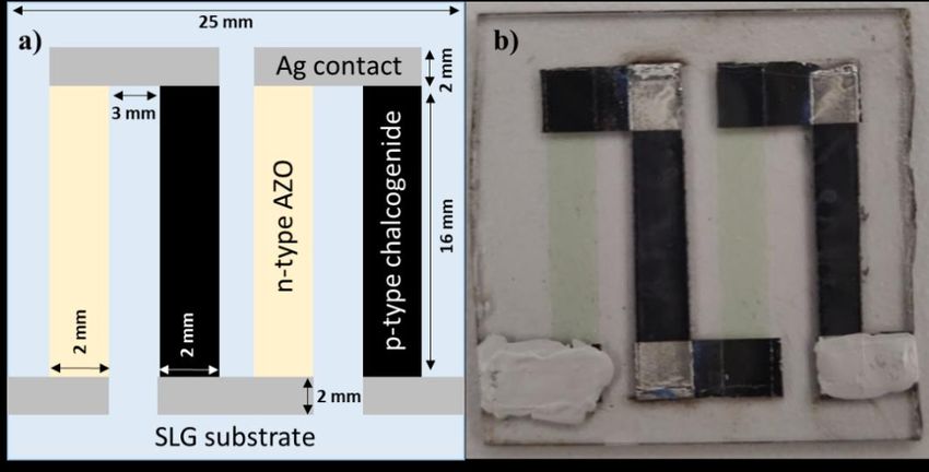
Al:ZnO-based thin films: a thermoelectric material for room temperature applications

 Gaetano Contento1, Marcello Massaro1, Francesca Di Benedetto1, Antonella Rizzo1
1
 ENEA, Brindisi Research Centre, Dept. of Sustainable Territorial and Production Systems - Division
of Materials Technologies and Processing for Sustainability, SS 7 Appia km 730, 72100 Brindisi - Italy
 *antonella.rizzo@enea.it

Al:ZnO (AZO) is a very interesting transparent n-type thermoelectric materials. If coupled with suitable
transparent p-type thermoelectric material it could open the way to the realization of a transparent
thermoelectric generator (TEG).
Al-doped ZnO thin films were deposited using a RF magnetron sputtering system in Ar+O2 atmosphere
by co-sputtering method with two distinct targets (ZnO and Al), where the Al percentage was varied
changing the power ratio between the two targets from 0.1 to 0.7.
Optical emissions (EOS) from the plasma during the deposition were measured using a high resolution
spectrometer in the wavelength range of 360-800 nm. EOS show that the constituents of each target were
successfully sputtered off. A plasma emission spectrum shows the presence of Zn+, Zn, Al and O
emission lines. The Zn and Al concentrations in the plasma can be calculated and correlated to Al:ZnO
thin films properties.
The structural properties of the realized films were characterized by X-ray diffraction measurements
performed under glancing incidence conditions.
Thermoelectrical and electrical characterizations were conducted in order to compare the response of
films grown under different conditions, using both specific chips as substrates for a Thin Film Analyzer
characterization – based on hot stripe method on suspended membrane – and glass substrates for a more
standard Van der Pauw configuration of measurement.
Optimal procedures were adopted to gain repeatability, accuracy and a better control of the systematic
errors. All measurements were performed in the temperature range of 20-50°C. The future efforts will be
devoted to pull up the temperature edge of characterization to prove stability of thin film performances.

 23
Comparative study on the thermoelectric properties of p-type CuI thin films

 F. Di Benedetto*, G. Contento, M. Massaro, B. Palazzo, L. Capodieci and A. Rizzo

 ENEA -- Italian National Agency for New Technologies, Energy and Sustainable Economic
 Development, Brindisi Research Centre, SS 7 Appia km 706, 72100 Brindisi, Italy,
 *francesca.dibenedetto@enea.it

Over the past few years, efforts have been made to develop new thermoelectric materials based on earth-
abundant, non-toxic and low-cost elements in order to boost the adoption of the thermoelectric technology
and foster its large-scale application. Copper iodide (CuI) is a material of recent interest for thin film
thermoelectric applications because it is a p-type candidate with performance equivalent to the currently
in market n-type material in term of optical transparency and electrical conductivity.
In this work we reported a comparative study on the thermoelectric properties of CuI thin films obtained
by physical evaporation of CuI commercial precursor - with or without subsequent iodination - or direct
iodination of Cu thin layers.
All the thin films were characterized to study the morphology, structure and chemical aspect of the
realized CuI thin films. Particular attention was focused on the thermoelectric, thermal and electrical
characteristics of the realized samples deposited onto pre structured chip and bare substrates by using a
thin film analyzer (TFA) equipped with HCS1 module.

 24
Mercoledì 16 Febbraio

SESSIONE 3: Thermoelectrics in enterprise applications
Chair: Valeria Demontis

 25
Cogeneration by a plug-in thermoelectric device integrated within a conventional solar-thermal
 system

 Marco Chiarappa1, Bruno Lorenzi1*, Fabio Fabbris1, Maurizio Miozza2
 1
 GemaTEG Italia Srl, Perugia - Italy
 2
 GemaTEG Inc, Bellevue WA, USA
 *bruno@gemateg.com

Low conversion efficiency and cost are the leading causes of thermoelectric generators' limited presence
in the marketplace. Integration in commercially viable solutions tailored to specific niches may address
the limitation of this technology, opening new opportunities in energy harvesting from renewable sources.
GemaTEG has developed an innovative plug-in device for cogeneration within a conventional thermal
solar panel. The system consists of vacuum tubes with thermosyphon able to harvest solar energy, and
store it in a dedicated reservoir though a heat transfer fluid. A thermoelectric harvesting chamber between
the thermosyphon condenser and the heat transfer fluid allows cogeneration of heat and electricity without
the complexity of moving parts.
The following presentation shares the methodology adopted for the system optimization, the experimental
data from the prototype, and several opportunities for improvement currently under evaluation. An
electrical conversion efficiency around 4% is within reach with commercial Bi2Te3 modules and
optimized thermosyphon configuration. Larger conversion efficiency requires more invasive approaches
to increase the absorber surface and minimize the loss while maintaining the system static (without
tracking devices). Furthermore, opportunities for cogeneration after sunset may further increase the
benefits.

 26
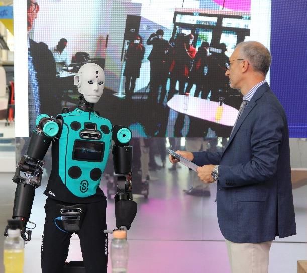
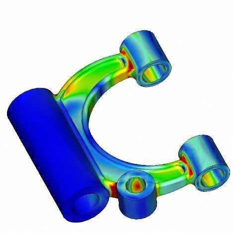
APPLICATION OF THERMOELECTRIC TEGS TO FUNCTIONAL SAFETY SYSTEMS OF
 ANTHROPOMORPHIC ROBOTS

 Fabio Puglia1,*, Wayan I Wayan Krisnayudi 2
 3
 Victor Ottolina,

 *fabio.puglia@iscsrl.it

In the context of the technological nowadays scenario, collaborative and anthropomorphic robotics
mainly, is increasingly assuming an operational role and effectiveness in supporting man in activities that
are not completely codified or replacing them in dangerous and tiring jobs. For this reason, ISC-Oversonic
started at the end of 2020 a Humanoid Robotics Project that is gaining increasing interest. One of the
main issues related to the management of the RoBee System is the management of thermal flows,
dissipation and power supply of safety sensors on board. In this last application slot, the use of
thermoelectric technologies can be strategic to continuously power the local safety sensors in accordance
with EN ISO 13849-1 and EN ISO 13849-2. The challenge is therefore to propose TEG as a certified
element of functional safety in advanced cobot systems.
The humanoid system is powered by 48V DC and has within it multiple electronic calculations mainly
responsible for computer vision and training of neural networks in edge-computing. The covering suit,
made of particular fibers to allow effective thermal insulation and to make the system completely
waterproof with IPX4 degree while determining critical issues in the management of thermal flows,
defines the operating envelope. The presentation therefore aims to show the operating conditions, the
safety of the safe mode (SIL 3 compliant to EN 60204-1) in the phases of human-machine interaction,
and how thermoelectric is used. In detail, the results of both the analytical simulations and the FEM
analysis will be presented. The TEGs were applied during the tests both using classic and flexible modules
with different temperatures range and heat exchanger characteristics. Heat decentralization was managed
through specially designed heat-pipes.

 27
Giovedì 17 Febbraio

SESSIONE 4: Computational approaches to materials design and
investigation
Chair: Simone Fabiano

 28
Strange Thermoelectrics

 Dario Narducci*

 Dept. Materials Science, University of Milano Bicocca, via R. Cozzi 55, 20125 Milano
 *dario.narducci@unimib.it

In addition to its most widespread metrologic application, thermoelectricity is commonly seen as a tool
either to convert heat into electric power or, conversely, to extract heat from a sink. This has somehow
concentrated research effort toward materials with high figures of merit according to the celebrated
paradigm of the electronic conductor – phononic glass. However, over the last years more exotic
applications of thermoelectricity have surfaced, in no way connected either to energy or temperature
measurements [1]. In this talk I will address a few of such ‘strange applications’, which could contribute
to further extend the interest toward thermoelectricity. Two study cases will be specifically considered,
connected to electrocatalysis and to chemical sensing.
Use of Seebeck effect to modify (improve) the catalytic activity of oxides have been reported by Huang
and coworkers [2]. The basic idea is to induce a shift of the Fermi level at the catalytic surface by applying
a controlled heat flux across the thermoelectric catalyst. In this way, electronic exchange responsible for
promoting a reaction at the surface is obtained. The effect is fully equivalent to that obtained by applying
an electric polarization across the catalyst, with the remarkable advantage of not needing porous electric
contacts to be deposited on the outer surface. Ideal thermoelectric catalysts are therefore materials
showing a large Seebeck coefficient and a low thermal conductivity – with no additional constraint on
their electrical conductivity. The approach has already found preliminary applications to hydrogenate
CO2 [2] and to produce hydrogen peroxide [3].
A similar use of the Seebeck effect may be conceived for chemical sensors. In chemoresistive devices, it
is well known how sensitivity is seldom an issue, while the real challenge is selectivity. The standard
approach to overcome the problem is to build up a matrix of sensors, feeding its response to some
numerical device (e.g. a neural network). A single chemical sensor may be used, instead, where the Fermi
energy is swept by modifying the temperature drop across it. A spectrum of its (electrical) response as a
function of Fermi energy is then obtained, witnessing its changing catalytic activity toward the
oxidation/reduction of the analyte. Applications of the so-called Seebeck sensors (not to be confused with
the gas sensors powered by TEGs) have been obtained, among others, to selectively detect hydrogen [4,
5] – quite a sensitive issue in view of the many uses of hydrogen both as an energy vector and for energy
storage.

References
 [1] Yang L, Chen Z-G, Dargusch MS, Zou J (2018) High Performance Thermoelectric Materials:
 Progress and Their Applications. Adv Energy Mater 8:1701797
 [2] Achour A, Chen K, Reece MJ, Huang Z (2018) Tuning of Catalytic Activity by Thermoelectric
 Materials for Carbon Dioxide Hydrogenation. Adv Energy Mater 8:1701430
 [3] Lin YJ, Khan I, Saha S, Wu CC, Barman SR, Kao FC, Lin ZH (2021) Thermocatalytic hydrogen
 peroxide generation and environmental disinfection by Bi2Te3 nanoplates. Nat Commun 12:180

 29
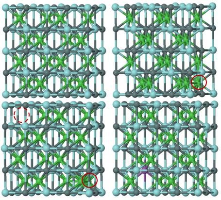
Ab initio study of bulk and defective ZrNiSn half-Heusler alloys

 E. Ascrizzi1*, C. Ribaldone1, L. Maschio1, S. Casassa1
 1
 Theoretical Chemistry Group, Dipartimento di Chimica, Università di Torino, Italy
 *eleonora.ascrizzi@unito.it

In recent years, thermoelectric (TE) materials have become of increasing interest, thanks to their
electronic and transport properties which make them very suitable as green energy sources. Among
different TE materials, the half-Heusler (HH) alloys are of particular interest for their excellent electronic
transport properties and their tunable band gap, which allow the possibility of tailoring TE efficiency.[1]
The presence of defects can enhance TE properties of alloys, but from an experimental point of view it is
always very difficult to establish the exact relationship between properties and atomic structure. This
knowledge would be of great importance, since it provides an indication on how to improve the
performances of thermoelectric materials. In this framework, ab initio study and characterizations of TE
materials can help to detect, evaluate and improve thermoelectric properties, by analyzing the bulk
structure and the role of defects in modifying the electrical conductivity and transport properties. While
TiNiSn-based alloys are now known as reliable thermoelectric materials,[2] there are still few
experimental measurements on ZrNiSn-based alloys, even though their Seebeck coefficients were found
to be higher than in the TiNiSn compounds.[3] At the same time, when these materials are used in the TE
generator devices, not only their thermoelectric properties, but also their thermal stability is very
important. ZrNiSn has good properties also in this respect, with a thermal stability higher than TiNiSn.[4,
5] Considering these promising features, we turned our attention to an ab initio characterization of
ZrNiSn-based alloys with the CRYSTAL code,[6] using DFT-PBE calculations and basis sets of localized
Gaussian orbitals. The obtained structural, electronic and thermoelectric properties for the pristine ZrNiSn
alloy are in good agreement with those reported in experimental studies, revealing a higher computed
power factor with respect to TiNiSn. Then, in order to build models consistent with experimental
samples,[7, 8, 9] three of the most likely point defects were simulated: (1) an interstitial Ni atom, (2) an
antisite and (3) a Sn/Sb substitution (see Fig. 1). The effect of these defects on the electronic properties
has been evaluated through the calculation of band structures and density of states. Both the interstitial
Ni and the antisite defect introduce states in the forbidden energy region, reducing the band gap and even
causing the system to be metallic if the defect concentration is high enough. The band structure of the Sb-
doped supercell shows a shift of the Fermi level toward the conduction band. This could lead to a possible
increase of the carrier concentration, σ and ZT. The transport properties calculated for the defective
systems will be shown, compared and commented, with the aim of clarifying the different mechanisms
and proposing the design of increasingly performing materials.

 30
Fig.1. Optimized structures of 2x2x1 ZrNiSn bulk and defective supercells. Pristine ZrNiSn (upper right
panel), interstitial Ni defect highlighted with a red circle (upper left panel), anti-structural defect: a red
circle highlights the interstitial Ni atom and a dashed red circle the vacancy (lower right panel),
substitutional defect: a Sn atom is substituted with a Sb atom, represented with a purple sphere (lower left
panel). Green spheres represent Ni atoms, cyan represent Zr atoms and gray represent Sn.

References

[1] X. Shi et al., Int. Mater. Rev., 61, 379-415, 2016
[2] A. Dasmahapatra et al., J. Phys. Chem. C, 124, 14997-15006, 2020
[3] H. Muta et al., J. Alloys Compd., 469, 50-55, 2009
[4] D. Jung et al., J. Alloys Compd., 489, 328-331, 2010
[5] X. Li et al., Research, 2020, 1-9, 2020
[6] R. Dovesi et al., WIREs Comput. Mol. Sci., 8, e1360, 2018
[7] Y. Tang et al., Energy Environ. Sci., 11, 311-320, 2018
[8] H. Miyazaki et al., Mater. Trans., 55, 1209-1214, 2014
[9] C. Fu et al., Adv. Sci., 7, 1902409, 2020

 31
Role of defects and secondary phases on the electronic structure and transport properties of
 thermoelectric TiNi1+xSn half Heusler compounds

 Alberto Castellero1,*, Francesco Aversano1, Mauro Palumbo1, Marcello Baricco1, Stefano Boldrini2,
 Alberto Ferrario2, Carlo Fanciulli3, Antti Karttunen4, Loredana Edith Daga1, Silvia Casassa1, Atreyi
 Dasmahapatra1, Lorenzo Maschio1
 1
 Università degli Studi di Torino, Dipartimento di Chimica & Centro NIS, Torino, Italy
 2
 CNR - ICMATE, Unità di Padova, Padova, Italy
 3
 CNR - ICMATE, Unità di Lecco, Lecco, Italy
 4
 Department of Chemistry and Materials Science, Aalto University, Finland
 *alberto.castellero@unito.it

The MNiSn (M = Ti, Zr, Hf) alloys were among the first half Heusler compounds to be characterized in
terms of thermoelectric properties (i.e., electrical resistivity and Seebeck coefficient). Since then, this
family of compounds has been extensively studied both from the experimental and computational point
of view, leading to the development of high performing thermoelectric materials (ZTmax = 1.5 at 820 K)
such as Ti0.5Zr0.25Hf0.25NiSn. Among half Heusler compounds TiNiSn is considered a model system for
understanding the relationship between structural, microstructural and thermoelectric properties.
According to the ternary phase diagram, the formation of TiNiSn half Heusler single phase from the melt
is hindered by a complex solidification path and requires long annealing time. A literature survey shows
that different samples of nominally stoichiometric TiNiSn have extremely scattered values of electrical
conductivity and Seebeck coefficient. Such a dispersion of data can be ascribed to residual secondary
phases and point defects, that affect the charge carrier concentration. On the one hand, the presence of
metallic secondary phases (e.g. TiNi2Sn, Ni3Sn4, Ti6Sn5, Sn) increases the charge carrier concentration in
the sample, raising the electrical conductivity and lowering the absolute value of the Seebeck coefficient.
On the other hand, point defects act as intrinsic dopants and their role on the electronic and thermoelectric
properties was investigated both experimentally and theoretically several authors. It was demonstrated
that a small excess of Ni leads to the partial occupancy of the Wyckoff position 4d (interstitial Ni defect)
expanding the cell, without precipitation of the full Heusler compound TiNi2Sn due to the slight solubility
of TiNiSn for Ni.
The above picture shows that, at the current stage, the understanding and control of both the role and
concentration of defects that deviate from the ideal crystal is far from complete. In this view, the aim of
this work is twofold. On the one hand, we investigate the role of punctual defects on the thermoelectric
properties of TiNiSn through DFT modelling. On the other hand, we compare the calculated
thermoelectric properties with the experimental values obtained for TiNi1+xSn samples in bulk form.
DFT calculations showed that the presence of both interstitial Ni defects and composition conserving
defects narrow the band gap with respect to the defect free structure leading to values that are comparable
to the experimental one. Accordingly, experimental investigations confirmed that interstitial Ni defects,
as well as metallic secondary phases, increase the metallic behaviour of the defective structure with
respect to the defect free structure, raising the electrical conductivity and lowering the absolute values of
the Seebeck coefficient.

 32
Impact of doping on the thermal conductivity of PEDOT and PEDOT:PSS through Molecular Dynamics
 simulations

 Paolo Sebastiano Floris1,*, Claudio Melis2, Riccardo Rurali1
 1
 Institut de Ciència de Materials de Barcelona (ICMAB-CSIC) Campus de Bellaterra,
 08193 Bellaterra, Barcelona, Spain
 2
 Dipartimento di Fisica, Università di Cagliari, Cittadella Universitaria, I-09042
 Monserrato (Ca), Italy
 *pfloris@icmab.es

Organic materials for thermoelectric applications have attracted a fair amount of attention in recent years
due to remarkable advances achieved in terms of their ZT (the thermoelectric figure of merit): a value of
0.42 has been reported by [1]Kim et al. for poly(3,4-ethylenedioxythiophene) polystyrene sulfonate
(PEDOT:PSS) films treated with dimethyl sulfoxide (DMSO), while 0.25 has been obtained for
PEDOT:Tosylate by [2]Bubnova et al. In this work we investigate various PEDOT and PEDOT:PSS
samples in both their neutral and doped (bipolaronic) state and with distinct concentrations of PSS through
Molecular Dynamics, by taking advantage of the all-atom force field recently developed by [3]Micheals
et al. In the case of bare PEDOT we find that changing the distribution of chain lengths affects the thermal
conductivity of neutral and doped samples in a different way: longer chain lengths result in higher
conductivities in the neutral scenario, whereas an intermediate chain length gives the highest value in the
bipolaronic case. The role of PSS and of its concentration is discussed in the bipolaronic case.

[1] G. H. Kim, L. Shao, K. Zhang, K. P. Pipe, Nat. Mater. 2013, 12, 719
[2] O. Bubnova, Z.U. Khan, A. Malti, S. Braun, M. Fahlman, M. Berggren and X.
Crispin, Nat. Mater. 2011, 10, 429
[3] W. Micheals, Y, Zhao, J. Qin, Macromolecules 2021, 54, 5354
This project has received funding from the European Union’s Horizon 2020 research and innovation programme
under grant agreement No 955837

 33
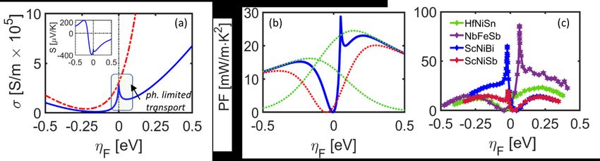
ElecTra: A Botzmann Electronic Tranport simulator for complex bandstructure thermoelectric
 materials

 Patrizio Graziosi1,2*, Zhen Li2, Neophytos Neophytou2
 1
 CNR – ISMN, Bologna
 2
 University of Warwick, School of Engineering
 *patrizio.graziosi@cnr.it

We introduce the open-source simulation code ElecTra (Electron Transport simulation lab), 1 which
computes the transport coefficients in bipolar complex bandstructure materials within the energy and
momentum dependent relaxation time approximation. We couple the Boltzmann transport method to DFT
bands for half-Heusler materials, considering both electron-phonon and ionized dopant scattering. The
full energy and momentum dependence of the relaxation times is essential in capturing the correct
transport features. 2-4

We then compare the conventional combination of unipolar transport coefficients with the simultaneous
consideration of the full bipolar effects in the calculation of the transport coefficients. A large difference
between the two treatments exists for narrow bandgap materials.
Lightly doped narrow gap semiconductors with asymmetric conduction/valence bands offer the
unconventional possibility to achieve extremely high thermoelectric power factors of up to 50 mW/mK2,
if they possess highly asymmetric conduction and valence bands in terms of density of states or phonon
scattering rates. This is achieved because, under these conditions, charge transport becomes phonon
scattering-limited, which allows large conductivities. Finally, we interpret related experimental findings.
5,6

References:
[1] https://github.com/PatrizioGraziosi/ELECTRA
[2] P. Graziosi, C. Kumarasinghe, N. Neophytou, J. Appl. Phys. 126, 155701 (2019).
[3] P. Graziosi, C. Kumarasinghe, N. Neophytou, ACS Appl. Energy Mater. 3, 5913 (2020).
[4] Z. Li, P. Graziosi, N. Neophytou, Phys. Rev. B 104 (19), 195201 (2021).
[5] P. Graziosi, N. Neophytou, J. Phys. Chem. C 125, 1168 (2020).
[6] P. Graziosi, Z. Li, N. Neophytou, Appl. Phys. Lett. under review.

 34
Figure1: (a) flow chart of the ElecTra code; (b) TiCoSb bandstructure; (c) constant energy surfaces from the TiCoSb valence band 0.12 eV below the band edge (blue), and other two surfaces from other band indexes at different energies, constructed by ElecTra code and represented in cartesian axes to compute the tensor components of the transport coefficients. The surfaces are represented as dots, each dot is a transport state. Transitions from the blue dots into the green/red dots can be the usual transitions in the case of an inelastic inter-band scattering event (i.e. absorption/emission of optical phonons). Figure 2: (a) electrical conductivity for very asymmetric conduction and valence bands in terms of effective masses (0.2 m0 and 1m0) and deformation potentials (3 eV and 6 eV) with a narrow bandgap of 0.4 eV at 900 K. The dash-dot red line is for the case when only scattering with phonon is considered (no with dopants). F = 0 represents the intrinsic Fermi level, the inset reports the Seebeck coefficient. (b) The peak in and the non-zero S in the intrinsic region, return an additional spike in the Power Factor (PF) which is a purely bipolar effect not captured by combining simple unipolar considerations, in dotted red lines and then combined in the green dotted line. (c) This effect is observed also in some narrow gap half-Heusler materials, reported in the legend, for T = 900 K. 35
First principles investigation of transport properties of 2D SnX2 (X=S, Se) and Janus SnSSe
 monolayer

 Himanshu Nautiyal 1, Paolo Scardi1*
 1
 Department of Civil, Environmental and Mechanical Engineering,
 University of Trento, Italy
 *
 E-mail of the corresponding author: paolo.scardi@unitn.it

Low-cost, earth-abundant, and environment-friendly materials have attracted the attention of the
thermoelectric community.[1] Recently, there has been a surge in the study of 2D materials for their
potential thermoelectric applications. Among the various studies, a recent report investigated the two-
dimensional Janus monolayers WS-X (X=Se, Te) for high thermoelectric performance.[2] Breaking the
structural symmetry plays a crucial role in tuning the electronic properties of 2D materials. Therefore, by
converting a monolayer structure into a Janus monolayer the electronic properties can be manipulated.
Tin-based chalcogenides show an interesting thermoelectric property and are earth-abundant.[3] SnX2
(X=S, Se, and Te) has a layered structure with space group P ̅m1. SnX2 monolayers can be converted
into a Janus monolayer by replacing the chalcogen atoms from the top or bottom layer with desired
chalcogen atoms.
We have investigated the electronic and transport properties of the SnS2, SnSe2, and Janus SnSSe
monolayer via density functional theory using Perdew-Burke-Ernzerhof exchange-correlation potential.
The systems were modelled with a vacuum of 15 Å to minimise the interaction with periodic copies. Due
to the presence of heavy Sn atoms, the effect of spin-orbit coupling (SOC) on the band structure was also
investigated. All three monolayers exhibited an indirect bandgap and band degeneracy at the Γ-point.
With the introduction of SOC, the splitting of the degenerate bands was observed. The dynamical stability
was investigated by calculating the phonon dispersion curve. The transport coefficients such as the
Seebeck coefficient, the electrical conductivity, the power factor, and the electronic thermal conductivity
were evaluated using the BoltzTraP2 code based on the Boltzmann transport theory within constant
relaxation time approximation. This study presents a systematic investigation of the electronic, transport
properties of the three monolayers.

 a) b) c)

 Schematic diagrams showing modelled monolayers a) SnS2, b) SnSe2,
References:
 and c) SnSSe
[1] X. Shi, L.
Chen, and C. Uher, “Recent advances in high-performance bulk thermoelectric materials”, International
Materials Reviews, 10.1080/09506608.2016.1183075, (2016)

 36
[2] Abhishek Patel, Deobrat Singh, Yogesh Sonvane, P.B. Thakor, and Rajeev Ahuja, “High
Thermoelectric Performance in Two-Dimensional Janus Monolayer Material WS-X (X = Se and Te)”,
ACS Applied Materials & Interface, 10.1021/acsami.0c13960, (2020)

[3] Shan Li, Xiaofang Li, Zhifeng Ren, and Qian Zhang, “Recent Progress on High Performance of Tin
Chalcogenides Thermoelectric Materials”, Journal of Materials Chemistry A, 10.1039/C7TA09941J,
(2018)

 37
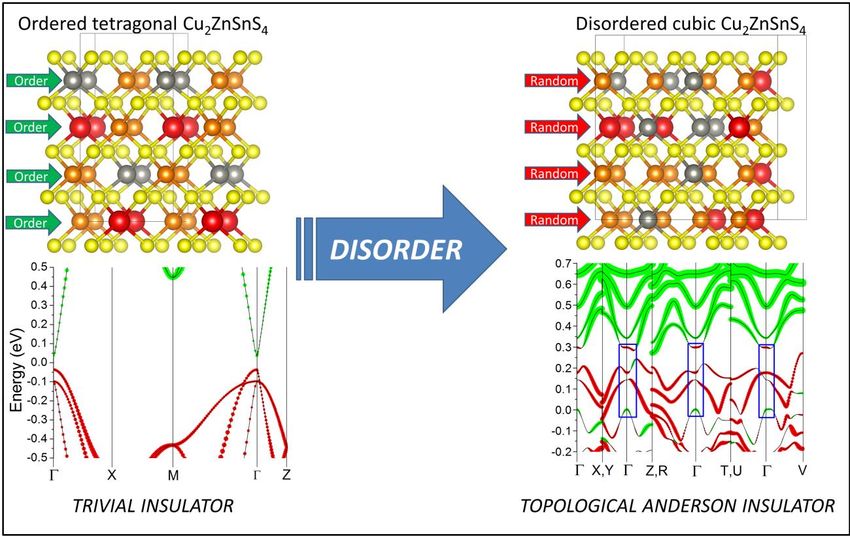
Topological Anderson Insulator in Cation-Disordered Cu2ZnSnS4

 Binayak Mukherjee1,*, Eleonora Isotta1, Carlo Fanciulli2, Paolo Scardi1
 1
 Department of Civil, Environmental and Mechanical Engineering, University of Trento, Via Mesiano
 77, 38123 Trento, Italy
 2
 National Research Council of Italy, Institute of Condensed Matter Chemistry and Technologies for
 Energy (CNR-ICMATE), Lecco Unit, Via Previati 1/E, 23900 Lecco, Italy
 *binayak.mukherjee@unitn.it

Using ab initio calculations supported by experimental transport measurements, we present the first
credible candidate for the realization of a disorder-induced Topological Anderson Insulator in a real
material system. High energy reactive ball-milling produces a polymorph of Cu2ZnSnS4 (CZTS) with
high cation disorder, which shows an inverted ordering of bands at the Brillouin zone center, in contrast
to its ordered phase. Adiabatic continuity arguments establish that this disordered Cu 2ZnSnS4 can be
connected to the closely related Cu2ZnSnSe4 (CZTSe), previously predicted to be a 3D topological
insulator. Band structure calculations with a slab geometry reveal the presence of robust surface states,
while impedance spectroscopy coupled with resistivity measurements point to the surface-dominated
transport which such states would imply; thus making a strong case in favor of a novel topological phase.
Disordered CZTS along with the closely related CZTSe show significantly improved thermoelectric
properties in low density, porous samples. This manifests as a reduction in thermal conductivity, enhanced
by low-lying optical modes, without the corresponding loss in electrical conductivity, due to surface-
dominated, scattering-resistant transport via the topological surface states. This potentially leads to a
phonon-glass-electron-crystal type system, allowing for the exploitation of topological features via
nanostructuring, to improve thermoelectric performance.

 38
Puoi anche leggere